Japan will be able to move forward to manufacture 2nm logic chips made by its chip venture Rapidus but developed by U.S. based IBM (NYSE:IBM) through a chip licensing agreement in late 2022 with IBM.
On May 6, 2021, IBM unveiled a breakthrough in semiconductor design and process with the development of the world’s first chip announced with 2 nm nanosheet technology – Gate-All-Around (“GAA”) – the next generation of transistor design that enables device scaling beyond today’s FinFETs. It is projected to achieve 45% better performance or 75% more energy efficiency than leading 7 nm chips.
Rapidus, a privately held Japanese chip venture established in August 2022 with a 7.3 billion Yen investment from eight major Japanese companies – NTT, NEC, Kioxia, Sony, Softbank, Denso, Toyota, and MUFG Bank, has ambitious plans to set up a prototype production line for cutting-edge 2nm semiconductors by the first half of 2025.
Their aim is to distinguish themselves as a foundry from other foundries such as TSMC (TSM), Samsung Electronics (OTCPK:SSNLF), and Intel (INTC). However, achieving this goal solely within Japan’s borders is a challenging task. Rapidus has already initiated a partnership with IMEC, a microelectronics research hub based in Belgium, to advance their semiconductor technologies collaboratively.
In contrast, Samsung made an announcement in mid-2022 about commencing initial production of its 3nm process node, implementing the GAA transistor architecture. The GAA process involves horizontally stacking multiple nanowires or nanosheets on top of each other, in contrast to the FinFET design, which necessitates placing multiple vertical “fins” side by side to enhance the flow of electricity, as depicted in Chart 1.
Imec
Chart 1 Source: IMEC
In the coming years, several major players in the semiconductor industry are gearing up for significant advancements:
- Samsung is planning to introduce its second-generation 3-nm chips in 2023 and intends to commence mass production of GAA-based 2-nm chips by 2025.
- TSMC (Taiwan Semiconductor Manufacturing Company) is also embracing GAA transistors, starting with its N2 process technology. They have set a timeline to transition their 2nm GAA process into production by 2025.
- Intel, under the brand name RibbonFET, is preparing to adopt GAA technology in its semiconductor manufacturing process at the 2-nm node, similar to TSMC’s strategy. Intel aims to launch GAA RibbonFET transistors by mid-2024.
The joint venture involving Rapidus holds great promise for Japan’s semiconductor industry resurgence. Of particular significance is the role Rapidus will play in revitalizing IBM as a formidable player in the chip sector, by commercializing the 2nm chip initially developed at IBM Research, the research and development division of IBM. IBM Research is one of the world’s largest industrial research organizations, with 12 labs spanning six continents.
To provide some context on IBM’s semiconductor business:
- IBM’s Bob Dennard is credited with inventing the DRAM memory chip in 1966.
- In 1993, IBM achieved $2.5 billion in sales from DRAMs, as well as ASICs (Application-Specific Integrated Circuits) and microprocessor chips. However, in 1999, IBM exited the DRAM business while continuing to offer ASICs and foundry services.
- Apple began using IBM’s PowerPC processors in 1994 but switched to Intel’s x86 design for its Mac computers in 2005.
- IBM divested its chip foundry business when it sold its IBM Microelectronics division to GLOBALFOUNDRIES (GFS) in 2014. IBM paid GFS $1.5 billion to assume its loss-making chip business and become IBM’s exclusive chip supplier for the following decade.
- In 2016, IBM Research introduced 7nm FinFET Technology featuring EUV (Extreme Ultraviolet) Patterning and Dual-Strained High-Mobility Channels, with prototypes produced at GFS.
- GlobalFoundries discontinued 7nm production in 2018, leading to a legal dispute with IBM in 2021 over the $1.5 billion payment and contract commitments.
The collaboration between Rapidus and IBM Research, combined with the resurgence of IBM’s chip-related endeavors, has the potential to significantly impact the semiconductor industry landscape.
Japan’s Semiconductor Industry in 2023
The transformation of Japan’s semiconductor industry over the past few decades is a notable case study. In the early 2000s, Japan faced a critical challenge in transitioning from vertically integrated semiconductor firms, which both designed and manufactured chips, to a more specialized model where companies either focused on chip design (fabless) or chip manufacturing (foundry).
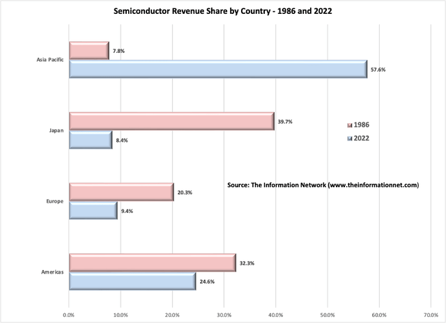
Chart 2 provides a striking visual representation of this transformation:
In 1986, Japan held a dominant 39.7% share of the global semiconductor market, which was valued at $28.4 billion at that time.
Fast-forward to 2022, and Japan’s share had dwindled significantly, accounting for just 8.4% of the global semiconductor market, which had grown to a staggering $574.1 billion.
This drop from nearly 40% to 8.4% is a significant decline compared to Japan’s status in the 1980s when it was the world’s largest semiconductor producer, commanding over 50% of global semiconductor production. This transformation reflects the shifting dynamics and challenges faced by Japan’s semiconductor industry as it adapted to evolving market demands and global competition.
The Information Network
Chart 2
Investor Takeaway
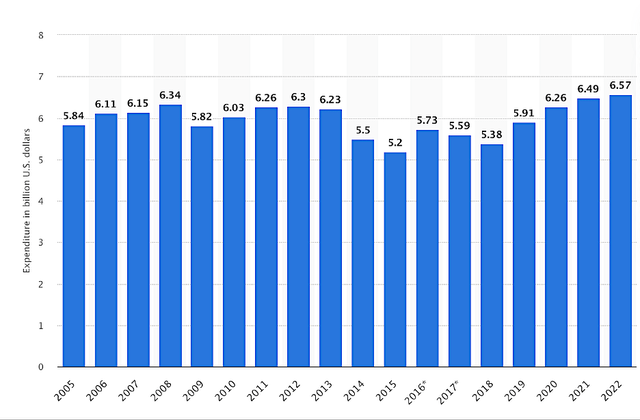
In 2022, IBM allocated $6.57 billion towards research, development, and engineering, as shown in Chart 3. The company maintains its position as one of the most prolific research-focused companies globally and consistently receiving a substantial number of patents in the United States. Despite its extensive patent portfolio, IBM consistently delivers innovative products and services. Many of IBM’s ongoing development initiatives revolve around hybrid cloud solutions, artificial intelligence (AI), blockchain, and quantum computing, reflecting the company’s commitment to advancing these transformative technologies.
IBM
Chart 3
The introduction of Japan’s own “Chips Act” to incentivize semiconductor companies to establish fabs within the country is a significant step in revitalizing its semiconductor manufacturing industry. The Japanese government’s approval of 774 billion yen ($6.8 billion) in funding for domestic semiconductor investment demonstrates a strong commitment to this endeavor.
One notable development is TSMC’s decision to build a chip plant in southern Japan, with support from Sony Group Corp and Denso Corp, each taking a minority stake in the venture. This investment is expected to commence production by late 2024, and there are even discussions of TSMC potentially constructing a second facility in Japan, in addition to their existing $8.6 billion facility under construction. These moves underscore Japan’s determination to reestablish itself as a leader in advanced semiconductor manufacturing.
Beyond its Chips Act, Japan is investing heavily in establishing the infrastructure to resuscitate its flagging semiconductor industry, and IBM will benefit. According to a July 2023 article in The Japan Times:
“Rapidus engineers have been dispatched to IBM’s Albany NanoTech Complex to design 2 nm mass production lines while its factory is being built in Hokkaido, accelerating the development process. The Japanese firm expects to invest ¥5 trillion ($35 billion) in its 2 nm project, roughly matching the annual outlay of TSMC and fellow leading chipmaker Samsung Electronics.”
Rapidus has a construction timeline with plans to finish the factory building by October 2024, followed by the launch of a pilot production line in April 2025 upon the installation of production equipment. Their objective is to achieve mass production of 2-nanometer semiconductors by 2027.
In addition to the large investment coming from Rapidus, IBM is equally interested in fostering the relationship as Japan expands its foothold in advanced node production.
IBM Japan’s Chief Technology Officer Norishige Morimoto noted in The Japan Times article:
“When it comes to 2 nm technology, we are focusing our efforts on Rapidus and investing a great deal of resources to this project, even sacrificing some capacity that we could have used in other research. We want Rapidus to succeed. We want it to contribute to a stable supply of the chips we and the world need. We won’t rule out any options as long as they match with our business needs.”
IBM Research used one of the first EUV machines in the world, located at Albany Nanotech, to accelerate EUV lithography development for production use below the 7nm node. But Rapidus will need an EUV system in Japan, and ASML (ASML) the sole supplier of EUV tools, has a tremendous backorder for these systems. United States, Taiwan, South Korea, and Intel’s fab in Ireland.
ASML has made the decision to create a semiconductor production support facility near Chitose City, Hokkaido, Japan, slated for operation in the latter half of 2024, coinciding with the construction of the Rapidus factory focused on achieving 2nm mass production.
Read the full article here


